











Infrastructure & pilot lines
European and national semiconductor infrastructure
Explore European pilot lines and Lithuania's consortium facilities through one entry point.
Pick yours
Service catalogue
Find the service your project needs
Filter by specialisation area or search by keyword. Every service opens a detail page with scope, equipment and contact information.
Semiconductor Design and Simulation Support through the ChipsC2-LT Access Node
This service supports users throughout the semiconductor design lifecycle, from concept definition and feasibility analysis to design, simulation, tape-out preparation and validation. The service operates in coordination with the EU Chips Design Platform, which provides access to electronic design automation tools, process design kits, IP libraries and fabrication pathways.
Technology and Tools Selection Consulting
This service supports the selection of suitable semiconductor technologies and design tools for specific product or system requirements. The assessment considers:
R&D Projects with Industry
This service supports joint research and experimental development projects with industry partners. It is directed towards the development of new products, technologies or functional prototypes.
ABC Modelling of Carrier Dynamics
This service provides ABC simulations based on carrier dynamics parameters. The simulations can provide information on recombination rates of individual radiative and non-radiative channels.
Integrated Circuit Design: ASIC, RFIC, MMIC, Analog, Digital and Power ICs
This service provides full-cycle integrated circuit design from technical specification to tape-out for fabrication. It covers analog, digital and mixed-signal solutions implemented using CMOS, GaN and SiC technologies.
RF and Microwave Circuit Design
This service provides RF and microwave circuit design, covering schematic development and physical layout optimisation.
Power Electronics Design
This service provides power electronics design using CMOS, GaN and SiC technologies. It supports development of:
Digital Circuit Synthesis and HDL Design
This service provides digital integrated circuit design and synthesis using VHDL and Verilog. It covers simple logic circuits as well as ASIC, FPGA and SoC solutions for industrial, communication and automation applications.
Computer-Aided Modelling of Integrated Circuits and RF Systems
This service provides modelling of integrated circuits and RF systems using industry-standard design and simulation platforms.
Electromagnetic Analysis for IC, RF and Microwave Systems
This service provides electromagnetic analysis to optimise integrated circuits, RF systems and microwave systems.
Layout Design and Verification
This service provides physical layout design for integrated circuits, considering technological and foundry requirements.
Tape-Out Management
This service supports the transition from IC design to manufacturing. It includes coordination of design data, layout files and documentation according to foundry specifications.
Test System Development
This service provides customised automated test equipment solutions for prototype ICs or modular systems.
Chip Testing
This service provides testing of bare wafers and packaged integrated circuits. Measurements are performed up to 26 GHz and evaluate electrical parameters and RF characteristics.
Failure Analysis of Integrated Circuits
This service determines root causes of non-functional or malfunctioning chips using electrical and RF testing methods.
System-Level Integration Consulting
This service supports integration of ICs into complex systems and final products. It includes analysis of:
Prototype System Development and Demonstration
This service supports the creation of demonstration prototypes and validation of technological solutions under real-world conditions.
Design Optimisation and Redesign
This service supports improvement of existing integrated circuits and systems. It includes:
Electrical Characterisation of Semiconductor Structures and Devices
This service provides I-V and C-V measurements of semiconductor structures and devices over the temperature range from -40 °C to 300 °C.
Carrier Drift Current Transient Profiling in Semiconductor Devices
This service provides profiling of carrier drift current transients and measurement of:
Defect Spectroscopy by Deep Level Transient Spectroscopy
This service provides defect spectroscopy in semiconductor structures and devices using deep level transient spectroscopy.
Contactless Defect, Recombination and Radiation-Damage Characterisation
This service group provides several contactless and photoelectric methods for semiconductor defect and recombination characterisation.
Response-Speed Measurements of Photodetectors and High-Voltage Switches
This service determines response speed of photodetectors and high-voltage switches using 10 ps pulsed excitations at 10 Hz repetition rate and 100 ps temporal resolution.
Wide Bandgap Semiconductors for High-Power and High-Frequency Applications
This service provides an integrated fabrication chain for prototyping active and passive microelectronic and plasmonic components on wide bandgap semiconductor platforms.
SMT Assembly and Serial Production Optimisation
This service supports optimization of prototypes for serial production within the Protolab Continental SMT centre at KTU.
Packaging – Substrate and Interposer Manufacturing: Circuit for Routing, Interconnections and Vias Manufacturing
This service provides advanced semiconductor packaging processes based on SSAIL, Surface-Selective Atomic Interface Layer, technology. It enables selective surface metallisation, redistribution layer formation and electrical interconnect fabrication on organic and inorganic dielectrics and semiconductors.
Manual Die Bonding
This service uses a Fineplacer PICO multi-purpose manual die bonder for high-accuracy assembly of semiconductor components.
Semi-Automatic Ultrasonic Wire Bonding
This service uses a semi-automatic thermosonic wire bonder to create electrical interconnects between semiconductor dies and packages or carriers.
High-Precision Positioning, Bonding and Advanced Packaging
This service supports physical realisation and integration of fabricated chips using high-precision positioning and bonding.
Chip-to-System Wire Bonding
This service provides automatic chip-to-system connectivity through thermosonic wire bonding for System in package (SiP) applications.
Hybrid 3D Ceramic Printing
This service supports creation of complex ceramic structures using hybrid 3D printing/stereolithography system for advanced electronics packaging, including:
Printed and Organic Electronics
This service enables production of thin-film prototypes featuring a materials deposition system capable of depositing of a wide variety of fluids including biological fluids, inorganic and organic conductives and photoresists.
Photoluminescence Spectroscopy
This service provides luminescence-related measurement and analysis using complementary luminescence spectroscopy setups.
Time-Resolved Spectroscopy in Picosecond Domain
This service measures small carrier diffusion coefficients of 0.001–0.1 cm²/s in double-side polished semiconductor materials.
Spatially Resolved Luminescence Measurement and Analysis
This service provides spatially resolved luminescence measurement and analysis using a confocal microscope.
Luminescence and Surface Morphology Measurement Using Scanning Near-Field Optical Microscopy
This service provides spatially resolved luminescence measurement and surface morphology analysis using scanning near-field optical microscopy. It supports simultaneous high-spatial-resolution optical imaging and surface morphology information.
Cathodoluminescence and Electron Microscopy Services
This service group provides electron microscopy, cathodoluminescence, EBIC, defect-density evaluation and data-analysis services.
Carrier Dynamics Characterisation in Wide and Narrow Bandgap Semiconductors
This service provides characterisation of non-equilibrium charge carrier dynamics in organic or inorganic, wide or narrow bandgap semiconductors.
Ultrafast Carrier Dynamics Characterisation
This service provides contactless, non-destructive characterisation of ultrafast photoinduced processes in semiconductor materials and devices. It is suitable for investigation of:
Carrier Diffusion and Lifetime Measurement
This service provides contactless, non-destructive characterisation of carrier diffusion, mobility, recombination and refractive-index dynamics in semiconductor materials. It is suitable for investigation of charge transport processes in semiconductor materials and devices.
UV-VIS-NIR Luminescence Measurements of Semiconductor Materials and Devices
This service measures:
Emission Decay Kinetics Measurements
This service provides time-resolved measurements of UV-VIS emission decay kinetics, including:
Quantum Yield Measurements
This service determines emission efficiency by measuring the ratio of absorbed to emitted photons in luminescent semiconductor materials.
Surface Morphology Measurement Using Atomic Force Microscopy
This service provides surface morphology measurement and analysis using atomic force microscopy. It supports investigation of:
End-to-End Optical Characterisation
This service combines:
High-Accuracy Alanine-Based Dosimetry
This service provides high-accuracy alanine-based dosimetry in the range from 1 Gy to 200 kGy.
Investigation of Sensors under Pulsed X-Ray Irradiation
This service provides characterisation of detectors and other devices exposed to short X-ray pulses of broad spectrum.
Molecular Beam Epitaxy Growth of Advanced III-V Semiconductor Heterostructures
This service provides atomic-level control of film growth under ultra-high-vacuum conditions. It is intended for production of complex heterostructures and quantum-scale architectures.
Prototyping of III-V Group Semiconductor Optoelectronic Devices
This service provides an end-to-end prototyping chain for active optoelectronic components based on III-V compound semiconductors. The examples listed are:
PIC Front-End Prototyping: Lithography and Precision Dry Etching
This service provides an integrated fabrication chain for prototyping active and passive photonic components on III-V or silicon-based platforms.
Femtosecond Laser Waveguide Fabrication and Glass Processing
This service provides an integrated fabrication and characterisation platform for photonic integrated circuits based on femtosecond laser processing in transparent materials, particularly glass substrates. It enables rapid prototyping of embedded optical waveguides and 3D photonic structures for telecom and sensing applications.
Monitoring System Development for Industrial Applications
This service provides investigation and development of monitoring or quality-control systems based on terahertz frequency technologies. Terahertz radiation can penetrate a range of non-conductive materials, including plastics, ceramics, textiles and composites, without causing damage. The service enables non-invasive inspection and real-time analysis of internal structures, defects and inconsistencies.
Photonic and MEMS System Development through Foundry Pathways
This service supports development of traditional semiconductors and specialised photonic and MEMS systems through design, prototyping and access to a network of foundry partners.
3D Printing according to Customer Drawings
This service provides 3D printing according to drawings provided by the customer.
Scientific Literature Review and Technology Landscape Analysis
This service provides structured scientific literature reviews and technology landscape analyses for SMEs, start-ups and research entities developing semiconductor-related products or projects. The service draws on the combined scientific expertise of all four ChipsC²-LT consortium partners — FTMC, VU, VILNIUS TECH and KTU — across the full range of semiconductor technology domains covered by the centre.
Feasibility Studies for Semiconductor Products and Solutions
This service provides technological and engineering feasibility studies for new products or solutions. The service assesses whether a concept can be implemented using CMOS, GaN or SiC technologies.
Advanced Semiconductor, Photonic, MEMS and Heterogeneous System Prototyping
This service supports the transition from initial conceptual design to physical realisation of advanced semiconductor, photonic, MEMS and heterogeneous integrated systems. The service focuses on prototyping-oriented development activities that bridge research concepts with manufacturable demonstrators and pilot-scale implementations. The activities include advanced integrated circuit design, photonic integrated circuit development, MEMS device prototyping, heterogeneous integration of electronic
Pilot lines
The Chips for Europe Initiative aims to expand and upgrade existing pilot lines, creating a robust infrastructure capable of advancing cutting-edge semiconductor technologies to higher maturity levels. These facilities will enable faster industrial adoption and commercial deployment of next-generation solutions.
The pilot lines will offer a unique environment for testing, experimentation, and validation of prototype systems that integrate breakthrough innovations (such as quantum technologies, artificial intelligence, and neuromorphic computing) as well as enhanced functionalities like security, energy efficiency, and integrated photonics.
By enabling real-time feedback from prototyping to design teams, these lines will allow engineers to refine and optimise design models before manufacturing, significantly shortening development cycles and reducing time-to-market.
All pilot lines will be accessible to stakeholders across the value chain on open and non-discriminatory terms. As world-class European assets, they will reinforce Europe's position as a key player in global semiconductor innovation and provide a strong foundation for enhanced international collaboration.

NanoIC
The NanoIC Pilot Line, coordinated by IMEC, is dedicated to pushing the boundaries of semiconductor innovation beyond the 2 nm technology node. As a key European infrastructure, it supports the advanced development and pre-manufacturing of next-generation integrated circuits, reinforcing Europe's strategic position in the global semiconductor landscape.
This pilot line accelerates R&D in nanometer-scale circuit technologies, directly addressing the challenges and demands of industry stakeholders. It plays a crucial role in supporting the European Union's ambition to remain competitive in high-performance, energy-efficient, and scalable chip design and fabrication.
The NanoIC Pilot Line operates as an open innovation platform, bringing together academic institutions, industrial partners, and research organisations. It facilitates the co-development, validation, and commercialisation of emerging technologies, while ensuring broad access under fair and non-discriminatory conditions.
Visit NanoIC
APECS
The APECS Pilot Line, coordinated by Fraunhofer (Germany), focuses on the development of advanced packaging and heterogeneous integration technologies that bring together diverse semiconductor materials, components, and functionalities within a single compact system.
As traditional monolithic scaling (Moore's Law) reaches its physical and economic limits, heterogeneous integration becomes essential to meet the demands of next-generation systems.
APECS leverages technologies such as System-in-Package (SiP), 2.5D and 3D integration, enabling the combination of digital, analog, RF, memory, and photonic elements in highly efficient and flexible architectures.
This pilot line supports the European semiconductor ecosystem by accelerating the path from research to industrial manufacturing, in line with the objectives of the Chips Joint Undertaking.
Visit APECS
FAMES
The FAMES Pilot Line, coordinated by CEA-Leti (France), is part of the Chips for Europe Initiative and focuses on advanced semiconductor technologies for analog, mixed-signal, and power electronics applications, key enablers of next-generation connected and intelligent systems.
At its core, the pilot line builds on Fully Depleted Silicon On Insulator (FDSOI) technology, which enables the development of high-performance, low-power, and cost-efficient circuits. FDSOI is particularly suited for edge computing, automotive systems, IoT, and secure electronics.
FAMES provides a pathway to industrialise innovative designs, bridging the gap between R&D and large-scale manufacturing. It plays a vital role in strengthening Europe's technological sovereignty by offering a robust platform for developing and validating advanced components under open and non-discriminatory access.
Visit FAMES
PIX Europe
PIXEurope is the fifth Pilot Line initiative launched through the European Chips Joint Undertaking, established under the European Chips Act, to accelerate the development of photonic integrated circuit (PIC) technology – a critical enabler for high-speed computing, communications, quantum information systems, and beyond.
It will be Europe's first fully integrated, distributed Pilot Line connecting the entire PIC value chain – from design and fabrication to integration, packaging, and testing – across multiple coordinated European sites within a unified and standardized framework.
With a budget of €400 million and the participation of 20 institutions from 11 European countries (Austria, Belgium, Finland, France, Ireland, Italy, Poland, Portugal, Spain, the Netherlands and the United Kingdom), PIXEurope will master key technology platforms spanning a broad range of materials – from silicon and silicon nitride to indium phosphide, lithium niobate, and beyond – while also supporting hybrid integration and the co-integration of photonic and electronic chips.
Through prototyping services, including Multi-Project Wafer runs, as well as access to advanced equipment and infrastructure, collaborative R&D projects, training and consultancy, the Pilot Line will serve companies of all sizes through a centralized open-access gateway.

WBG Pilot Line
The WBG Pilot Line, based in Catania (Italy) and developed in collaboration with Tampere University (Finland), is one of Europe's key initiatives for advancing wide bandgap (WBG) semiconductor technologies. It focuses on the development, integration, and packaging of new high-performance, durable, and energy-efficient materials for next-generation power and RF applications.
Tampere University plays a leading role in the development and testing of WBG devices, including their integration into hybrid System-in-Package (SiP) architectures. This enables the creation of compact and robust solutions for demanding environments.
The pilot line supports the industrialisation of WBG materials and components for applications such as:
- Electric motor controllers
- Battery management systems
- Solar inverters
- 5G network base stations
In parallel, advanced techniques for SiP fabrication are being developed to enable full system integration, a crucial step toward reinforcing Europe's competitiveness and sustainability in the global semiconductor market.
Visit WBG Pilot LineAccess to Infrastructure
The Lithuanian Chips Competence Centre (ChipsC2-LT) provides unified access to a network of cutting-edge semiconductor R&D facilities across four leading national institutions – FTMC, VU, VGTU, and KTU.
Facilities include high-grade ISO 5-7 clean rooms, molecular beam epitaxy (MBE) and chemical vapor deposition (CVD) systems, electron-beam lithography, laser processing systems, and advanced characterization tools.

Atomic Layer Deposition
Atomic layer deposition (ALD) is a thin-film deposition technique that builds materials one atomic layer at a time through sequential, self-limiting surface reactions. This precise process enables uniform coatings on complex surfaces and supports key advances in electronics, energy technologies, and advanced materials.
Download PDF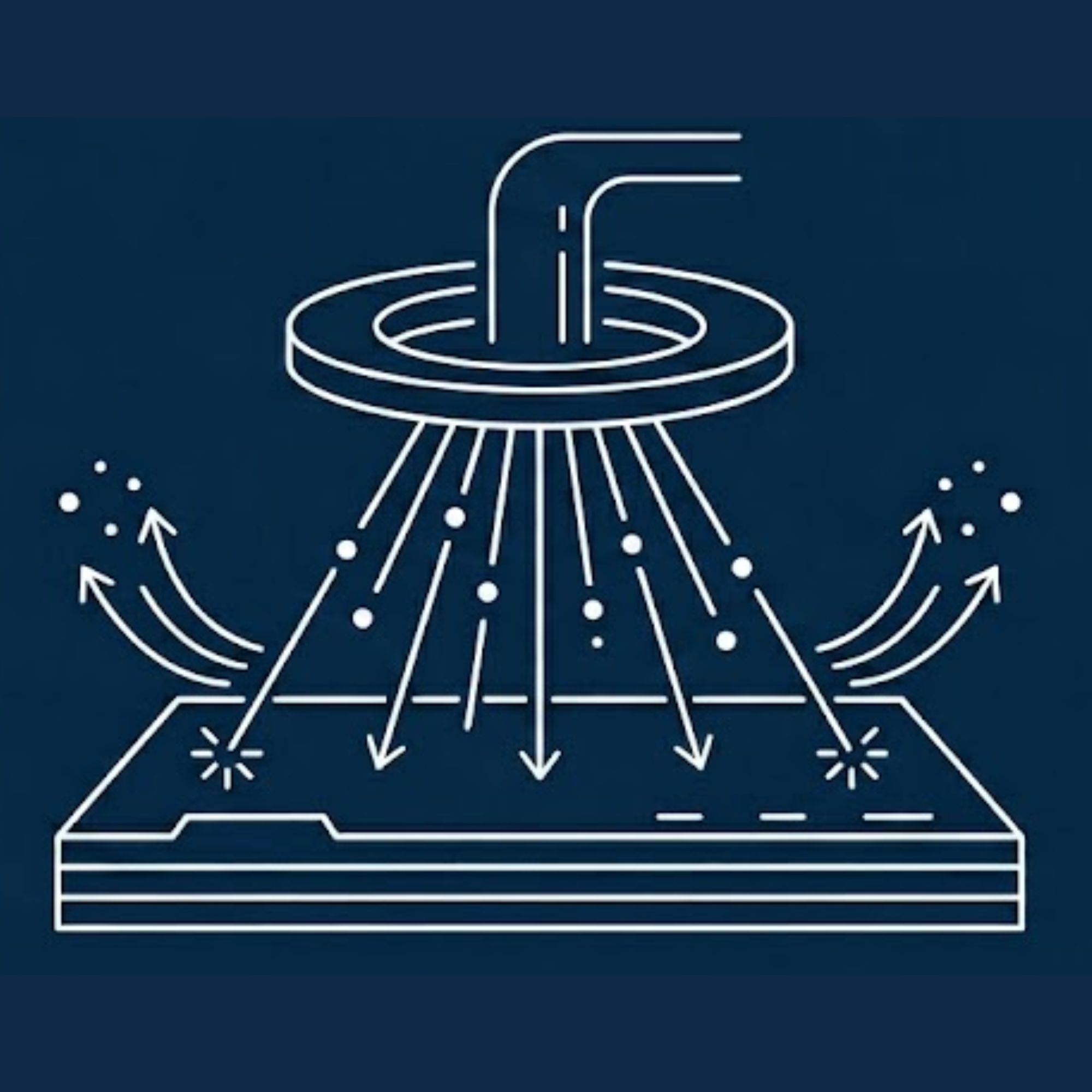
Oxygen Plasma Cleaning
Oxygen plasma cleaning is a plasma-based surface treatment that effectively removes organic contaminants using reactive oxygen species, improving surface cleanliness and wettability without damaging the substrate. It is widely used in micro- and nanofabrication to enhance adhesion or clean samples prior to processes such as deposition or lithography.
Download PDF
Plasma-Enhanced Chemical Vapor Deposition
Plasma-Enhanced Chemical Vapor Deposition (PECVD) is a versatile thin-film deposition technique that uses plasma to enable low-temperature growth of high-quality dielectric and semiconductor films.
Download PDF
Dry Etching
Dry etching is a plasma-based process that delivers precise, directional material removal through RF-activated reactive gases, offering superior control compared to wet etching. It is ideally suited for high-precision micro- and nano-fabrication.
Download PDF
Lithography
Lithography is a micro- and nano-fabrication process used to create precise patterns on various substrates. Combined with etching or lift-off process it enables the fabrication of features like trenches, vias, and metal layers. The Lithuanian Chips Competence Centre (ChipsC2-LT) offers three primary lithography techniques through its partner institutions.
Download PDF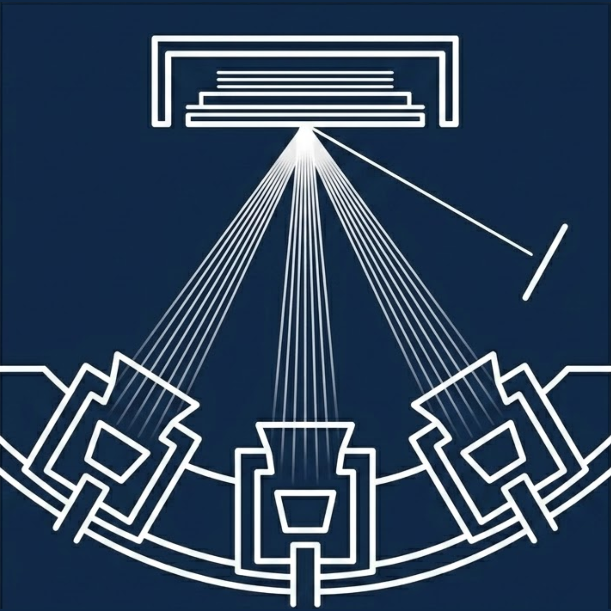
Molecular Beam Epitaxy
Epitaxial growth is a semiconductor fabrication technique used to grow highly ordered crystalline layers on a substrate with precise control over thickness, composition, and material quality. These properties are critical for the performance of microelectronic, power, and optoelectronic devices.
Among the main methods, liquid-phase, vapor-phase, and molecular beam epitaxy (MBE), MBE is particularly important for research and advanced device development. It enables atomic-level control of growth under ultra-high vacuum, making it ideal for complex heterostructures and quantum-scale architectures that drive innovation in next-generation semiconductor devices.
Download PDF
Die Bonding
Die bonding is a critical semiconductor assembly process used to mount a die (chip) onto a substrate, package, or wafer with high spatial precision. Utilizing advanced optical alignment and controlled thermal or force application, it enables reliable electrical, thermal, and mechanical connections for complex microelectronic, optoelectronic, and flip-chip architectures.
Download PDF
Magnetron Sputtering
Physical vapour deposition (PVD) is a family of vacuum-based techniques that convert a solid source material into a vapour to form thin films on a substrate. Magnetron sputtering is one of the main PVD methods, using energetic ion bombardment to eject atoms from a target material onto the substrate. This versatile process supports a wide range of metal, oxide, and dielectric coatings across research and industrial applications.
Download PDF
Metal-Organic Chemical Vapor Deposition
Metal–Organic Chemical Vapor Deposition (MOCVD) is a precise thin-film epitaxial growth technique in which metal–organic precursors react on a heated substrate to form high-quality semiconductor layers. It is widely used to produce advanced materials for optoelectronic and electronic devices.
Download PDF
Rapid Thermal Annealing (RTA)
Annealing in semiconductor manufacturing is a critical thermal process used to repair crystal damage and activate dopants, ensuring reliable device performance. A widely used technique is Rapid Thermal Annealing (RTA), where wafers are briefly heated above 1000 °C and cooled rapidly. This minimizes unwanted dopant diffusion, allowing the formation of shallow junctions essential for modern miniaturized devices. Compared to conventional furnace annealing, RTA offers faster processing, precise temperature control, and improved uniformity, making it indispensable for high-performance integrated circuits.
Download PDF
Wire Bonding
Wire bonding is a critical semiconductor fabrication technique used to establish electrical connections between integrated circuits (ICs) or other semiconductor devices and their package leads or substrates. Utilizing a combination of heat, pressure, and ultrasonic energy (thermosonic bonding), this precise process enables reliable electrical interconnects essential for microelectronic, power, and optoelectronic device packaging.
Download PDF
Electron-Beam Evaporation
Physical vapour deposition (PVD) is a family of vacuum-based techniques that convert a solid source material into a vapour to form thin films on a substrate. In electron-beam evaporation, a focused electron beam heats a source material in a crucible until it vaporises, and the vapour then travels through the vacuum chamber and condenses onto the substrate. Because the beam heats the source material directly, this method works well even for materials that are difficult to deposit by other means, and the deposition rate can be adjusted across a wide range, from slow and precise to fast and high-throughput. This makes it well suited to metal, semiconductor, and dielectric coatings for microelectronics and optics.
Download PDF
Surface Mount Technology
Surface mount technology (SMT) is a printed circuit board manufacturing technique used to place and bond electronic components onto a PCB with precise control over alignment, solder deposition, and thermal profile. The process combines three core stages: solder paste is first printed onto the board's pads, components are then placed onto the paste with precise alignment, and the assembly is finally heated in a reflow oven to melt the paste and form permanent solder joints. Together, these systems support PCB assembly across prototyping and low- to high-volume manufacturing.
Download PDF
Ion-Beam Sputtering
Physical vapour deposition (PVD) is a family of vacuum-based techniques that convert a solid source material into a vapour to form thin films on a substrate. In ion-beam deposition, an ion source generates a focused beam of energetic ions that strikes a target material, ejecting atoms so they can travel across and settle onto the substrate. Because the ion beam is generated independently of the target, its energy and direction can be controlled very precisely, which helps produce dense, well-adhered coatings. This makes it well suited to optical and protective coatings, including metal-oxide layers and diamond-like carbon films.
Download PDF
Electronic Design Automation Software
VILNIUS TECH and Kaunas University of Technology provide a comprehensive design and research environment for CMOS and GaN integrated circuits and advanced electronic systems. Comprehensive services cover the entire microelectronics development cycle, from system-level modelling and schematic creation to layout, verification, and fabrication-ready data generation. The team operates with industrial-grade EDA tools and process design kits (PDKs).
Download PDF