

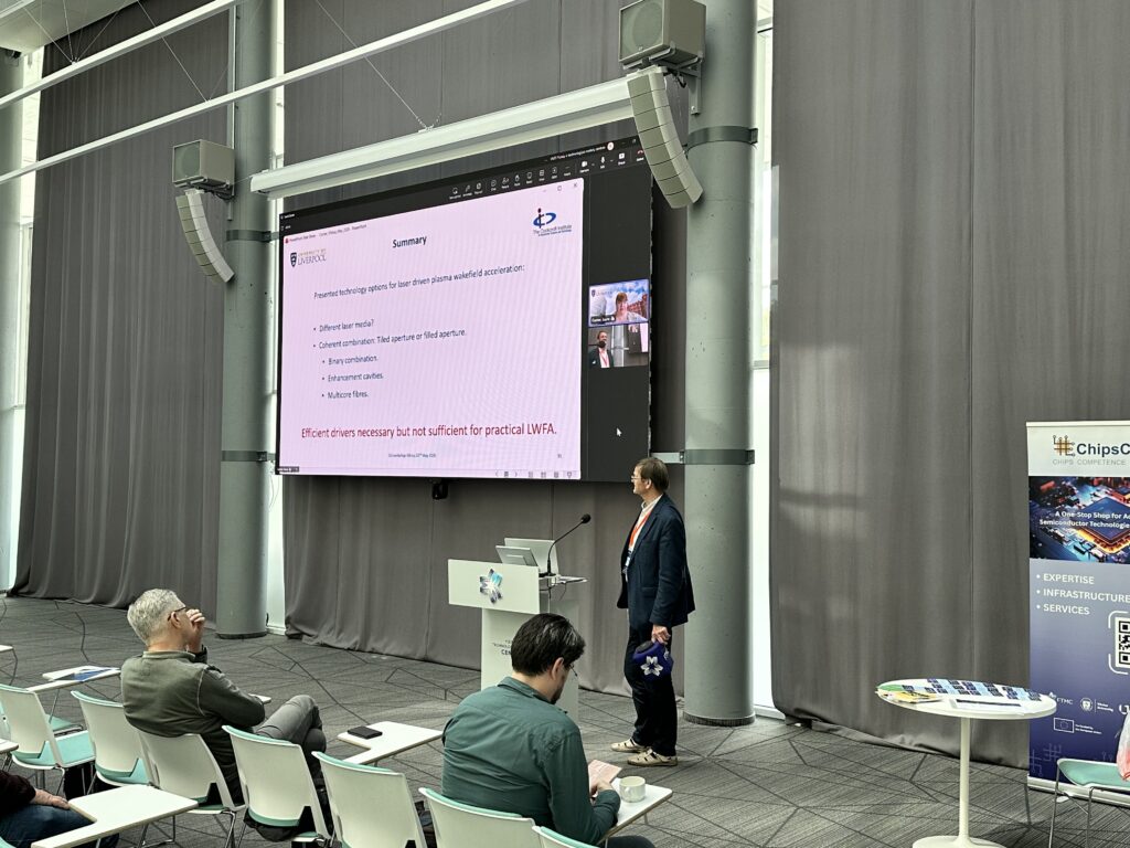
On May 21–22, the Center for Physical Sciences and Technology (FTMC) in Vilnius hosted the international workshop “Laser-Driven Particle Accelerators, Their Applications and Experimental Opportunities within the ELI Infrastructure.” The event brought together leading researchers from across Europe to discuss the latest advances in laser-driven particle acceleration, high-field physics, and emerging applications in science, medicine, and advanced technologies.
Beyond accelerator science, the workshop strongly highlighted the increasing importance of photonics technologies within the future semiconductor ecosystem, an area where Lithuania is rapidly strengthening its international position.
ELI Infrastructure Creates New Opportunities for Semiconductor and Photonics Research
Representatives from the three major Extreme Light Infrastructure (ELI ERIC) facilities, ELI Beamlines (Czech Republic), ELI-NP (Romania), and ELI ALPS (Hungary), introduced advanced open-access research infrastructures available to international scientific teams.
The presented experimental platforms included:
- laser-driven X-ray sources,
- neutron generation systems,
- accelerated electron and proton beams,
- advanced plasma-based acceleration technologies.
These capabilities open new opportunities for Lithuanian researchers working in laser technologies, semiconductor physics, photonics, and materials science.
Semiconductor Technologies at the Core of Advanced Laser Experiments
A particularly relevant presentation for the semiconductor community was delivered by researchers from Vilnius University’s Department of Semiconductor Physics. Their presentation, “Semiconductor Detectors for High-Energy Particles and Beams,” focused on advanced silicon-based detector systems used for precision measurements of laser-accelerated particle beams.
The presented technologies demonstrated how semiconductor devices are becoming essential components of modern laser and accelerator infrastructures.
Importantly, semiconductor detectors are not only used in experiments, they are increasingly fabricated and processed using ultrafast laser technologies themselves. Femtosecond laser processing enables highly precise structuring of silicon and wide-bandgap semiconductor materials, creating a strong technological link between photonics and semiconductor manufacturing.
Photonics as a Strategic Enabler for the Semiconductor Industry
Today, photonics technologies play a critical role across the entire semiconductor value chain. From extreme ultraviolet (EUV) lithography used in advanced chip fabrication to laser-based wafer processing, defect inspection, and optical metrology systems, modern semiconductor manufacturing would not be possible without photonics.
At the same time, semiconductor technologies are increasingly integrating photonic components directly into chips to enable:
- high-speed optical interconnects,
- energy-efficient data transmission,
- photonic integrated circuits (PICs),
- next-generation sensing and communication systems.
This convergence of photonics and semiconductors is becoming one of the key technological directions shaping the future of Europe’s semiconductor industry.
ChipsC²-LT Strengthens Lithuania’s Semiconductor Ecosystem
The topics discussed during the ELI workshop directly align with the strategic priorities of Lithuania’s Chips Competence Centre – ChipsC²-LT.
Coordinated by FTMC together with national and international partners, ChipsC²-LT supports the implementation of the European Chips Act initiative in Lithuania and aims to strengthen national semiconductor competencies in several key areas:
- chip design,
- power electronics,
- heterogeneous integration,
- photonic integrated circuits (PICs).
By leveraging Lithuania’s internationally recognized expertise in lasers, photonics, and THz technologies, the initiative contributes to building a highly specialized semiconductor ecosystem capable of supporting both research and industrial innovation.
Building Europe’s Future Through Semiconductor and Photonics Innovation
The ELI workshop clearly demonstrated how semiconductor technologies, laser systems, accelerator science, and photonics are increasingly converging into a single multidisciplinary innovation ecosystem.
Lithuania’s long-standing strengths in photonics create strong foundations for developing advanced semiconductor technologies and expanding Europe’s technological sovereignty in strategically important sectors.
Initiatives such as LASER PRO and ChipsC²-LT play an important role in transforming scientific excellence into practical semiconductor innovation, industrial competitiveness, and long-term economic growth.